• New organic conductive materials, which can be mixed into inks and printed onto substrates, are now being used to produce flexible electronics.
• IoT devices, medical applications, and foldable screens: organic semiconductors, which are being used in a growing number of applications, also have the advantage of being less harmful to the environment.
“Organic materials are printable: they can be incorporated into inks and then deposited on a substrate by printing.”
The development of the electronics industry relies on minerals, mainly silicon, which is currently in short supply, and, to a lesser extent, germanium. At the same time, it also depends on rare earth metals whose limited availability now amounts to a major geostrategic challenge, which is obliging manufacturers to restrict their use and to seek out alternatives.
In February 2023, a team of American scientists published an article in the Journal of the American Chemical Society reporting on the development of an organic conductor with properties that rival those of traditional indium compounds, produced with a polymer ink composed of widely available carbon-based materials. In Brittany, France, technology company Asca has developed an organic photovoltaic film, which does not contain rare earth metals or silicon. Both of these technologies rely on the use of conductive and semi-conductive organic materials, in particular polymers, which could soon provide an alternative to traditional semiconductors. Already used to make transistors, photovoltaic cells and light-emitting diodes, organic conductive materials, which benefit from flexibility and printability, are relatively easy and inexpensive to produce. They are also paving the way for a new approach to electronics, known as organic electronics.
Organic semiconductors also have the potential to break new ground in the field of artificial intelligence
Polymers are chemical substances composed of macromolecules (molecules made up of thousands of similar atoms), which occur naturally or can be obtained in a laboratory process known as polymerisation. Cellulose (wood, paper, cotton, etc.), plastics and rubber are among the best known polymers, most of which are electrical insulators. However, a number of polymers discovered in the late 1970s are conductive, and their development is now paving the way for the new field of organic electronics and a host of printed and flexible devices.
Organic electronics also has the potential to break new ground in the field of artificial intelligence by integrating sensing, memory and processing functionalities, which are separate in traditional systems In April 2023, a team from the universities of Hong Kong and Xi’an Jiaotong published an article in Nature in which they described a new type of organic electrochemical transistor capable of acting as a sensor and processor, which has the potential to improve the performance and energy consumption of electronic devices.

OLED highlights the potential of organic electronics
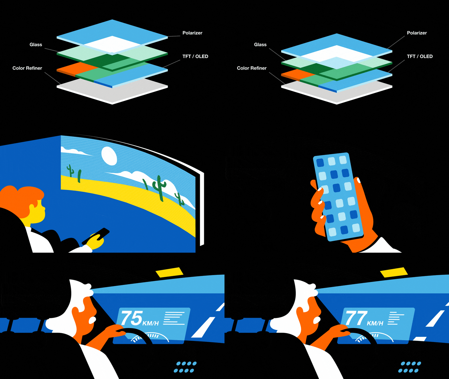
OLED (Organic Light-Emitting Diode) technology used in telephone screens and digital cameras has already familiarised the general public with organic semiconductors. Organic light-emitting diodes are optoelectronic devices capable of emitting light when an electric current flows through them. They notably enable OLED screens to be self-emissive or to display images without a backlight unit, which reduces the number of manufacturing stages for these displays along with the quantity of raw materials required for their production. Two major advantages over the previous generation of screens that used liquid crystal display (LCD) technology.
Thinner, lighter, and more flexible, OLED screens offer more intense colours, deeper blacks, better contrast, wider viewing angles and greater responsiveness. Curved, foldable and rollable models are also possible. To quote the French National Centre for Scientific Research (CNRS): “In view of these characteristics OLED technology may well be destined to dominate the market.” However, the process used to produce OLED displays, which are increasingly in demand, remains costly and labour intensive. Several research projects are underway to explore alternative production techniques, notably methods to produce solution-processed OLEDs, which can be used to build larger displays without the industrial constraints of traditional OLEDs.

A new manufacturing process for electronics
In July 2023, the Indian Institute of Science announced that it had developed a composite semi-conductor containing 40% polymer that can be used to print flexible screens for foldable phones and other devices. Printability is a key advantage of organic materials, which can be deployed in the form of inks and deposited on substrates. Electronic circuits can be printed using a variety of techniques (inkjet, screen printing, engraving, flexography, etc.). The resulting production processes are simpler and less costly than electronic lithography, which is the main technique used for silicon-based components.
Another advantage of this manufacturing process is that it can be used with both rigid substrates, such as glass, and flexible substrates, such as plastics, textiles and paper, making it possible to integrate a wide range of electronic devices – sensors, for example – into objects of any shape, size or composition.

A wide range of applications
The development of printed organic semiconductors will pave the way for numerous applications including:
- photovoltaic cells on flexible films that can cover any surface (for example, vehicle body work)
- portable devices for sports and healthcare markets, in particular biomedical sensors for remote patient monitoring. Also in healthcare, there are new materials that may be used to treat blindness, notably photovoltaic retinal prostheses which can convert light into electrical signals that are relayed to patients’ brains
- integrated sensors in floors, walls and industrial machinery and components that can measure temperature, humidity, pressure, deflection, etc.
- smart packaging and labels to protect product integrity, ensure traceability and quality control, and prevent counterfeiting.
In Belgium, global adhesives giant Henkel has teamed up with the SME Quad Industries to accelerate the development and marketing of printed semiconductor applications. In 2020, the two partners worked together to develop medical patches for the monitoring of coronavirus patients. Today they are exploring a range of further uses for their technology in healthcare (patches to monitor epileptics), sports (flexible sensors to be inserted in golfers’ shoes), and the building industry (leak detectors), etc.
Piezotech, a subsidiary of French chemicals group Arkema, produces electroactive polymers, which change in size and shape when stimulated by an electric field, in the form of powders, inks and thin films. In the framework of the European project Supersmart, the company has presented two prototypes based on these high-potential materials: an intelligent shock detection label, which can be used to track parcels and fragile objects or measure wear and tear on equipment, and an anti-counterfeiting label.

An environmentally friendlier technology?
In the context of a growing scarcity of raw materials and the ongoing ecological crisis, are organic semiconductors more sustainable? The French Printed Electronics Association (Afelim) argues that they can contribute to reducing the environmental impact of a number of sectors. Low-temperature manufacturing processes used to produce organic semi-conductors consume less energy and raw materials. What’s more, they also offer solutions for environmental challenges posed by today’s technologies, such as the management of electronic equipment waste. Another potential benefit is their integration into industrial parts for the purposes of predictive maintenance. The Industrial Technical Centre for Plastic and Composite Innovation (IPC) and the CEA (French Alternative Energies and Atomic Energy Commission) are developing a plastic film with in-built sensors, which is integrated directly into the composite materials used to produce wind turbine blades. The new technology is designed to detect any potential damage to the blades with a view to extending their lifespan.
Organic semiconductors can also be integrated into clothing and implanted in the human body for medical applications, which is why they are described as biocompatible. At the same time, most of them are also biodegradable.
The twin advantages of organic semiconductors, printability and flexibility, have made organic electronics a promising sector. According to research firm IDTechEx, this emerging market is set to grow from $41.2 billion in 2020 (around €36 billion) to $74 billion in 2030 (over €65 billion). Over the next few years, this new disruptive technology will likely to be used in a growing number of applications alongside silicon-based electronics.
Sources
Flexible, Printed and Organic Electronics 2020-2030: Forecasts, Technologies, Markets https://www.idtechex.com/en/research-report/flexible-printed-and-organic-electronics-2020-2030-forecasts-technologies-markets/687
Demain, l’électronique flexible ? (Are flexible electronics the future?) https://lejournal.cnrs.fr/articles/demain-lelectronique-flexible
L’électronique organique imprimée à l’heure de la maturité (“Printed organic electronics reach maturity”) https://www.cea-tech.fr/cea-tech/Pages/2021/L-electronique-organique-imprimee-a-l-heure-de-la-maturite.aspx
L’électronique organique, une révolution ? (“Organic electronics: a revolution?”) https://youtu.be/hA1YLADsBhw
L’électronique imprimée se rêve en championne des technologies vertes (“Printed electronics: a new champion for green technology”) https://www.industrie-techno.com/article/l-electronique-imprimee-se-reve-en-championne-des-technologies-vertes.61704


